Beyond SiC: The Case for Diamond in the Next Semiconductor Leap
- Blog
- Insights
-
Sep 04
- Share post
Beyond SiC: The Case for Diamond in the Next Semiconductor Leap
The Relentless Drive for Progress
Semiconductor materials have always faced performance ceilings – thermal limits, switching losses, and breakdown voltages that eventually constrain mature technologies. Silicon is nearing these limits in high-power and high-frequency applications. While wide-bandgap (WBG) materials like SiC and GaN have extended performance, their physical and economic constraints are becoming clear at scale. As the industry seeks transformative gains, diamond is emerging as a serious candidate for the next materials breakthrough.
What sets today’s innovation pace apart is its speed. Semiconductor development, once slow and linear, now advances through global collaboration, rapid prototyping, and high-throughput experimentation. This acceleration shortens development cycles but adds pressure on supply chains, process stability, and reliability. Scalable, application-driven development is now essential for any new material to succeed.
Each generational shift has required not only scientific discovery but also readiness in manufacturing – especially surface preparation, defect control, and wafer scalability. These enabling technologies, though often behind the scenes, are crucial for moving materials from lab to market.
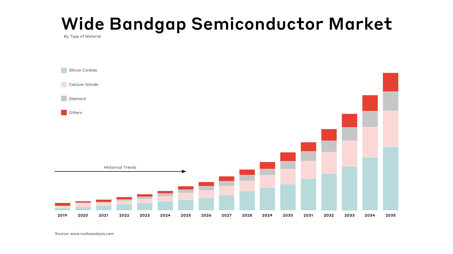
From Silicon to SiC – An Evolution in Bandgap
Silicon’s dominance stemmed from its abundance, manageable bandgap (1.1 eV), and compatibility with established processes. It powered CMOS logic and moderate – voltage devices across industries. However, rising demands for higher voltages, faster switching, and better thermal performance – particularly in automotive, industrial, and renewable sectors – exposed silicon’s limits. Silicon carbide (SiC), with a wider bandgap of ~3.3 eV, offered higher breakdown fields, elevated temperature operation, and superior thermal conductivity, making it ideal for power electronics (Tian et al., 2021). Early challenges included substrate defects, polytype control, and limited wafer size, all of which impacted device reliability.
Advances in physical vapor transport (PVT) growth, defect reduction, and 4H-SiC substrate quality made high-volume manufacturing viable. The introduction of 150 mm and 200 mm wafers further improved scalability. Controlled epitaxial growth enabled devices like trench MOSFETs and Schottky diodes (Kimoto & Cooper, 2014).
Processing also evolved. SiC slicing, grinding, and planarization required specialized tooling and CMP processes to ensure surface integrity and downstream yield. Close collaboration with surface technology experts refined polishing suspensions, pads, and cleaning techniques to meet these demanding specifications.
The Diamond Promise
As semiconductor demands push beyond the limits of SiC, attention is now turning to diamond – a material that could redefine what is possible in performance and durability. Diamond offers the most extreme semiconductor properties: an ultra-wide bandgap of 5.5 eV, thermal conductivity over 2000 W/mK, high carrier mobility, radiation hardness, and chemical stability (May, 2000; Isberg et al., 2013). These properties make it an ideal candidate for next-generation high-power, high-frequency, and harsh-environment electronics.
Yet significant hurdles remain. High-quality diamond is grown via microwave plasma-enhanced CVD on HPHT seeds—a slow, costly process with small substrate sizes. While polycrystalline diamond is more scalable, grain boundaries degrade performance.
Doping presents another challenge. While boron enables p-type conductivity, n-type doping remains inefficient due to deep donor levels (>0.5 eV), preventing the creation of effective p–n junctions (Umezawa et al., 2023). Surface processing is equally complex. Diamond’s hardness makes conventional grinding and CMP inadequate for the ultra-smooth finishes required. Recent advances in chemo-mechanical polishing with controlled oxidation and soft pad systems offer promising results but require precise control to avoid defects (Zhu et al., 2021).
For diamond to succeed, breakthroughs in scalable, reproducible surface processing are essential. Research into wafer-scale planarization, metrology, and defect control is gradually enabling the material’s potential (Balmer et al., 2009).
Looking Forward – From Theory to Practice
Diamond’s remarkable properties have been demonstrated in the lab, but commercial use faces obstacles in scalability, integration, and cost. Unlike silicon or SiC, diamond requires new approaches across the value chain – from growth to doping, metallization, and packaging.
In the near term, diamond’s key role is as a passive thermal management layer. GaN-on-diamond architectures leverage its exceptional thermal conductivity to improve heat dissipation and reliability in RF and high-frequency devices (Isberg et al., 2013).
Active devices – Schottky diodes, MOSFETs, and field-effect transistors – have been built, but the absence of efficient n-type doping prevents full CMOS circuits (Umezawa et al., 2023). For now, diamond suits unipolar or hybrid designs, particularly vertical devices capitalizing on its high breakdown field.
Processing challenges persist. Wafer uniformity, defect control, and precise surface finishing remain key hurdles. Metrology for detecting subsurface defects is still developing, and scaling to larger wafer sizes demands both material innovation and refined process control.
Research groups and industrial consortia are advancing automated polishing, closed-loop feedback, and hybrid chemo-mechanical techniques adapted to diamond’s unique wear behavior (Chicot et al., 2024). These innovations are enabling early wafer-scale prototyping.
Ultimately, diamond’s future depends on integrating into existing semiconductor ecosystems without requiring complete process overhauls. Like SiC, it will likely evolve through steady improvements in substrate quality, automation, and packaging—driven by expertise in ultra-hard material processing.
Pureon’s path
As a preeminent manufacturer of precision surfacing consumables for a wide assortment of materials, Pureon is actively working on new products to meet the challenges in processing diamond substrates. Developing new pads and slurries for diamond requires careful tuning of abrasive particle types, sizes, and chemistries to effectively remove material from this ultra-hard surface.
Most crucial is the balance of material removal rate with surface roughness to avoid subsurface damage and preserve diamond quality. It’s a very challenging process, but one for which Pureon is uniquely qualified to tackle given its unique experience manufacturing diamond abrasives and also developing consumables for other hard materials such as sapphire and SiC.
References
Balmer, R. S., Brandon, J. R., Clewes, S. L., Dhillon, H. K., Dodson, J. M., Friel, I., … & Scarsbrook, G. A. (2009). Chemical vapour deposition synthetic diamond: Materials, technology and applications. Journal of Physics: Condensed Matter, 21(36), 364221. https://doi.org/10.1088/0953-8984/21/36/364221
Isberg, J., Gabrysch, M., Twitchen, D. J., & Whitehead, A. J. (2013). Diamond for electronic devices. Semiconductor Science and Technology, 28(8), 085011. https://doi.org/10.1088/0268-1242/28/8/085011
Kimoto, T., & Cooper, J. A. (2014). Fundamentals of Silicon Carbide Technology: Growth, Characterization, Devices and Applications. Wiley.
May, P. W. (2000). Diamond thin films: A 21st-century material. Philosophical Transactions of the Royal Society A: Mathematical, Physical and Engineering Sciences, 358(1766), 473–495. https://doi.org/10.1098/rsta.2000.0531
Tian, R., Ma, C., Wu, J., Guo, Z., Yang, X., & Fan, Z. (2021). A review of manufacturing technologies for silicon carbide superjunction devices. Journal of Semiconductors, 42(6), 061801. https://doi.org/10.1088/1674-4926/42/6/061801
Umezawa, H., Makimoto, T., & Shikata, S. (2023). Progress and challenges in diamond semiconductor devices. Japanese Journal of Applied Physics, 62, SC0802. https://doi.org/10.35848/1347-4065/acf9f2
Zhu, T., Li, X., & Guo, D. (2021). Polishing of synthetic diamond substrates: Advances and challenges. Precision Engineering, 68, 126–134. https://doi.org/10.1016/j.precisioneng.2020.12.003