Semiconductors have revolutionized the way we work, communicate, travel, entertain, harness energy, and treat illness. They not only make useful devices of our daily life possible, but also make them more compact, less expensive, and more powerful.

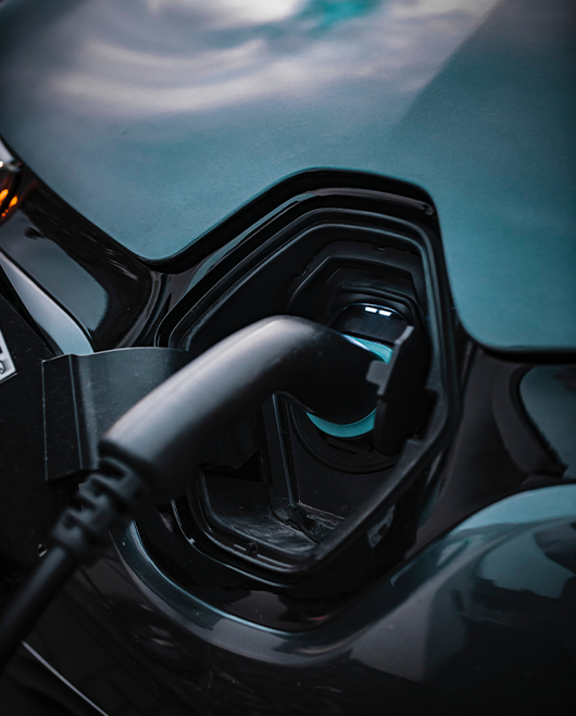
New technical advancements and requirements necessitate the use of silicon carbide (SiC) for many demanding semiconductor applications. Due to its physical and electronic properties, SiC based devices are well suited for high temperature and high-power/high-frequency electronic devices enabling the advancements in Electric Vehicles (EVs), 5G and IOT technologies. While they bring a lot of benefits for the end-user, the production of high-quality SiC substrates presents many challenges to wafer manufacturers.

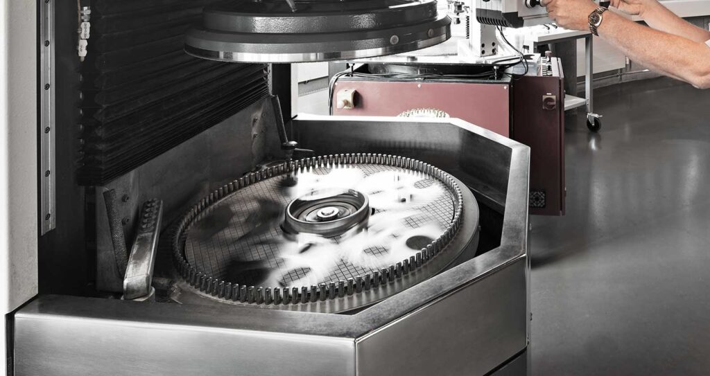
Pureon has been providing state-of-the-art solutions to SiC wafer manufacturers for over 15 years in the various process steps of slicing and surface finishing.Pureon supports manufacturers to establish reliable and efficient processes.
For further information, please contact us
we are happy to share our knowledge with you.

Dipl.-Ing. Helge Willers
Industry Expert Electronics & Semiconductors
+41 71 686 60 61
hwillers@pureon.com

Terry Knight
Industry Expert Electronics & Semiconductors
+1 620 321 3114
tknight@pureon.com